Six-Sigma in silicon carbide substrate manufacturing
 -
04. November 2022
-
3D measurement and inspection
-
04. November 2022
-
3D measurement and inspection
Six-Sigma in silicon carbide substrate manufacturing with LOTOS 3D
measurement systems.
Achieving the stringent zero defect strategy in the automotive industry is becoming a major challenge for silicon carbide substrate manufacturers. Both the switch from 150 to 200 mm wafers and the general shift in their focus away from pure silicon are making manufacturers struggling to achieve sufficient yields and reliability.
SiC is a combination of silicon and harder carbide materials, and its wide bandgap has made it a key technology for battery-powered electric vehicles. Silicon carbide operates at higher power, higher temperatures and higher switching frequencies than silicon. These properties can be used to increase the range of electric vehicle batteries and reduce charging time.
"People want to charge their cars in less than 10 to 15 minutes, and that's going to continue to evolve," said Sam Geha, CEO of Infineon Technologies' Memory Solutions. "That requires silicon carbide and other technologies, as well as more automation."
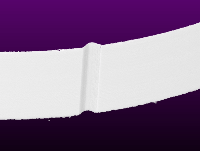
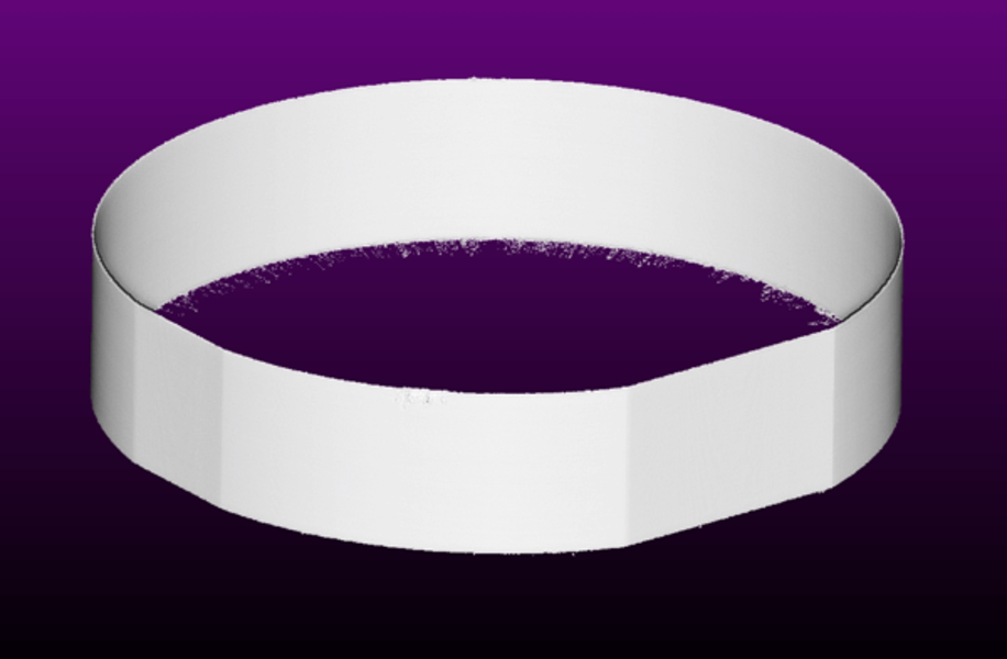
LOTOS 3D measurement systems help implementing the zero-defect strategy toward high-yield production processes without any scrap. Shortly after crystal growing, silicon carbide boules can be inspected for geometric sizes, eliminating scrap in subsequent production processes.
LOTOS checks all common parameters such as outer diameter and diameter at the primary and secondary flat, the flat lengths, the notch contour, as well as their exact angular positions.
Comments are disabled for this post.
0 comments